Project title: Tunable RESOnant SENSors based on multi-layer substrate integrated waveguide technology
Acronym: ResoSens
Program: Information and Communication Technologies
Project category: Experimental-demonstrative
Contract No. 399PED/2019
Project duration: 2020 - 2022
ResoSens Results
ACHIEVEMENTS Resonant sensor for measuring light intensity
Fig. 1. Photo of the resonant sensor assembly for measuring light intensity: the solar panel (a) is used as basic sensing device (a) connected to the microwave assembly (b) with the resonance frequency proportional to the light intensity incident on solar panel surface. The complete structure of the resonant sensor for determining the intensity of light radiation is shown in Fig. 1, where the two constituent elements are shown: (i) the solar panel (a), which is the actual sensor of the system, and (ii) the tunable SIW resonant circuit with varicap diodes. It can be seen that the microwave circuit associated with the sensor has a compact structure, due to the use of removable SIW circuit assembly. The determination of the microwave operating frequency (rejection) of the resonant structure dependence on light intensity was performed by connecting it to a wideband vector network analyzer (VNA). Sensor characterization was performed by exposing the solar panel to a light source with uniform and controlled light intensity distribution (ORIEL LSH-7320 ABA LED solar simulator). Since the light intensity available from the solar simulator (between 0.1 - 1 sun) proved to be too high for our solar panel model, a 50 dB broadband optical attenuator was inserted in between. |
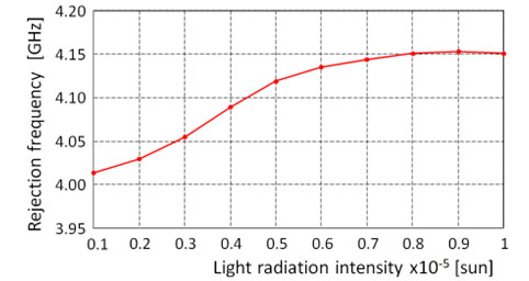
Fig. 2. Frequency response of the sensor shown in Fig. 1 vs light radiation intensity. The measured minimum (3.9794 GHz) and maximum (4.1509 GHz) resonance frequencies for the sensor indicate a deviation of 137.2 MHz, i.e. a relative bandwidth of operation of about 4.22% obtained for the light intensity variation between 10-6 sun and 10-5 sun (Fig. 2).
Fig. 3. Assembly of three electromagnetically coupled SIW circuits providing multiple frequency tuning possibilities, with visible intermediate tuning circuit (a), and after complete assembly, for microwave measurements with various load impedance (ZL) values (b). An experimental model with complex assembly of three coupled SIW circuits is shown in Fig. 3. Functionally, the intermediate coupled SIW circuit, actually a three LaTE structure [Details] is used for step-wise change of the structure’s operating frequency. The upper SIW circuit is provided with an SIW-CPW transition at the end of which any SMD component can be assembled, the type and value of which simulates the behaviour of a high-frequency sensor with reactive behaviour.
Fig. 4. Dependence of the rejection frequency of the circuit in Fig. 3 on type and value of load impedance ZL. |