
NANOMATERIALS ENABLING SMART ENERGY HARVESTING FOR NEXT-GENERATION INTERNET-OF-THINGS
Type of the project: Prizes for participation in Horizon 2020 |
NANO-EH project has received funding from the European Union’s Horizon 2020 Research and Innovation Programme under Grant Agreement No. 951761 |

The NANO-EH project was chosen in the FET Proactive: emerging paradigms and communities call (FETPROACT-EIC-05-2019) in the subtopic "Breakthrough zero-emissions energy generation for full decarbonisation".
| Results, stage 3 | Results, stage 2 | Results, stage 1 | Dissemination |
Results, stage 3
In Year 3 of the project, all the envisaged objectives for each activity have been fulfilled. The most significant achievements in 2023 are the following:
1. the patch antennas were characterized in microwaves on a high resistivity silicon substrate, with an air cavity under each antenna according to the design specifications, guaranteeing at the same time the mechanical robustness and an easy manipulation of the structures. The reflection coefficient is better than -12 dB at 24 GHz, and the gain measured at 24 GHz is approx. 4 dBi;
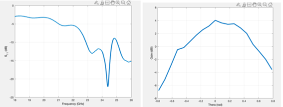 |
Reflection coefficient (left) and gain at 24 GHz (right) of the patch antenna on the silicon multilayer with an air cavity. |
2. the energy harvesters with an operating frequency between 24.25 and 27.50 GHz, on a high-resistivity silicon substrate, integrated with the power conversion unit, were tested. The DC voltage at the output of the rectifier network has a maximum value of approx. 25 mV between 23.75 GHz and 24.60 GHz for an input power level of -10 dBm;
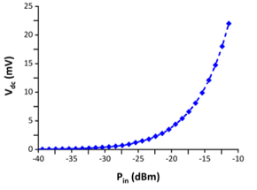 |
DC voltage at the output of the rectifier network, as a function of the input power level. |
3. the dissemination activity included 6 papers in ISI journals and 3 papers presented/to be presented at 3 international conferences. A paper in an ISI magazine was awarded with "Front cover", and a paper presented at an IEEE conference was awarded with "Best Student Paper Award"..
Results, stage 2
In Year 2 of the project, all the envisaged objectives for each activity have been fulfilled. The most significant achievements in 2022 are the following:
1. we designed and simulated (using a 3D electromagnetic tool and a circuit simulator) a rectenna and an array of rectennas with operating frequency in the band 24.25–27.50 GHz. The simulated maximum radiation efficiency for the whole rectenna array is about 43% for an input power level of about 14 dBm, which corresponds to an output differential voltage of 6.7 V on a 3.9 kΩ load;
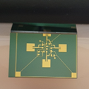
Top view of the 4 square patch antennas on silicon multi-layer with an air cavity under each antenna.
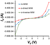
2. we designed and modelled theoretically a MIM diode based on dielectric and ferroelectric hafnium oxide, using QuantumEspresso and the software package Quantum Atomistic Toolkit (Q-ATK). This model has the potential of providing very useful information about the metal-oxide interface characteristics and allows estimating accurately the tunnelling current of a MIM diode;
I-V characteristics for the 3 optimized MIM diodes
3. we fabricated rectenna arrays with operating frequency between 24.25 and 27.50 GHz, on high-resistivity silicon substrate, integrated with their power control units. We managed to find the optimal solution to create an air cavity under each rectenna according to the design specifications, which guarantees at the same time mechanical robustness and an easy manipulation of the structures;
Detail with a section of a single rectenna array, in which one can see the air cavity under the rectennas.
4. the dissemination activity has comprised 1 ISI journal paper (Critical Reviews in Solid State and Materials Sciences, IF 11.178, CiteScore 19.6) and 4 papers presented at 2 international conferences (20th International Balkan Workshop on Applied Physics and Materials Science, and 2022 IEEE MTT-S International Conference on Numerical Electromagnetic and Multiphysics Modeling and Optimization – NEMO).
In the next and last year, we will characterize at microwaves the fabricated rectenna arrays to demonstrate the EM energy harvesting in the 24 GHz band.
_____________
Results, stage 1
In Year 1 of the project, all the envisaged objectives for each activity have been fulfilled. The most significant achievements in 2021 are the following:
1. at IMT we fabricated by ALD thin films (thickness of 7 nm) of ferroelectric hafnium oxide (HfO2) doped with zirconium (Zr). A detailed characterization has been carried out to confirm the ferroelectric properties of the obtained films, like GI-XRD, PFM and P-E polarization curves (material polarization as a function of the applied electric field). All the performed measurements have proven the ferroelectric characteristics of the HfO2 thin films (like the coercive field EC = 1 MV/cm, which is typical for this material.
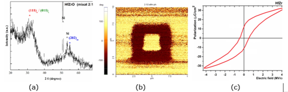 |
|
|
2.Thin films (7 monolayers) of molybdenum disulfide (MoS2) have been deposited by ALD-CVD on 4-inch wafers of Al2O3/HRSi and on 2-inch wafers of Al2O3/“c-cut” sapphire. The reproducibility of the ALD-CVD process is excellent. The thickness of the obtained MoS2 has a high degree of uniformity, with the thickness depending on the growth time: 1.2 nm in 0.3 hours, 3 nm in 0.75 hours, 5 nm in 1.25 hours, and 10 nm in 2.5 hours. Raman characterization confirmed that the deposited MoS2 is made of 7 monolayers and the policrystalline nature of the ALD-CVD MoS2, with crystalline domains around 20 nm.
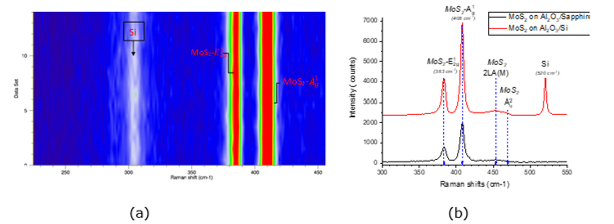 |
(Left) Micro Raman 3D imaging of 7-monolayer MoS2 deposited on Al2O3/HRSi substrate; (right) the characteristic Raman spectrum of 7-monolayer MoS2 grown on Al2O3/HRSi (red curve) and on “c-cut” sapphire (black curve). The phonon mode for the Si substrate is also observed at around 520 cm-1. |
3. For the PFM characterization of MoS2 thin films on silicon oxide (SiO2)/high-resistivity silicon (HRSi), we used samples purchased by 2D Semiconductors (dimensions of 1 cm x 1 cm, monolayer MoS2 on SiO2/HRSi, thickness of 300 nm/500 μm, respectively). We extracted the out-of-plane effective piezoelectric coefficient d33eff by analyzing first the responses obtained when sweeping the bias voltage along one direction (i.e., from 0 V to -10 V), and then by analyzing the curves obtained when sweeping the bias voltage along the opposite direction (from -10 V to 0 V).
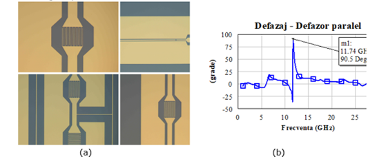
4. The fabrication of simple test structures to verify the properties of ferroelectric and 2D materials (in DC and at high frequencies) comprised: phase shifters based on ferroelectric hafnium oxide and planar diodes based on MoS2. In the case of the phase shifters, the experiments have demonstrated that the frequency-dependent phase shift for a maximum DC bias voltage of 4 V is excellent in the X band (8-12 GHz), with a maximum value of over 90 degrees at 11.74 GHz, whereas a “planar diode” based on monolayer MoS2 with a distance of 4 μm between the two golden contacts behaves as a p-type semiconductor diode (a possible cause for this could be ascribed to the doping occurring in the monolayer MoS2 during fabrication). These preliminary experimental results validate the ferroelectric nature of HfZrO thin films and the semiconducting behavior of monolayer MoS2, which represents the necessary prerequisite to fulfill the final objectives of the project. Moreover, the technological flux has been proven to be reliable and reproductible for the following steps.
(a) Phase shifters fabricated on a HfZrO/HRSi wafer; (b) frequency-dependent phase shift.
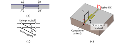
5. In Year 1, a bow-tie antenna has been designed and simulated for “energy harvesting” applications in the 24 GHz ISM band (Industrial, Scientific, Medical), which covers the frequency range 24–24.25 GHz. The complete structure of the layout for the harvesting circuits comprises a bow-tie antenna, a MoS2-based diode, a bifilar line section to connect the antenna to the spur-line, the RF-rejection circuit, and transmission lines and pads for the RC load circuitry. The optical and nano-lithographic masks for both bow-tie antennas and diodes have been already fabricated, and the technological process has been accurately verified for the next steps.
(a) Layout of a spur-line; (b) equivalent circuit of a spur-line; (c) electromagnetic model proposed to decouple the RF and DC signals.
6. The dissemination activity has comprised 2 papers in ISI journals (IEEE Transactions on Microwave Theory and Techniques, IF 4.381, CiteScore 8.1; IEEE Nanotechnology Magazine, CiteScore 4.2), 2 papers accepted for oral presentation at 2 international conferences (International Microwave Symposium – IMS2021 and PIERS2021), and a workshop organized within the international conference International Semiconductor Conference – CAS2021.
____________________
Estimated results
The estimated result is a rectenna with operating frequency in the band 24.25-27.50 GHz, able to rectify tens of millivolts (typical value) or, equivalently, tens/hundreds of microwatts (typical value).
We list hereinafter the goals to be achieved for each part of the rectenna:
- a planar antenna (dipole / bow-tie / patch) on high-resistivity silicon substrate, with operating frequency in the band 24.25-27.50 GHz and radiation efficiency of at least 75%. The radiated field will be broadside or end-fire;
- a rectifying diode, of two (2) types, i..e, a MIM diode, based on hafnium oxide, with an area of some square microns, oxide with a thickness of some nanometers, and cutoff frequency over 60 GHz, or a planar geometrical diode, based on molybdenum disulfide, fabricated by means of nanolithography techniques. In both cases, the diode should be able to rectify a DC voltage of tens of millivolts;
- an antenna-diode matching network;
- a DC circuit (typically comprising a DC-DC converter and a storage capacitor).
