Laboratory of Micro/Nanophotonics
Head of the Laboratory: Dr. Dana Cristea
Objective ICT-2009.3.9: Microsystems and Smart Miniaturised Systems
Target outcomes:
a) Heterogeneous Integration
c) Application-specific microsystems and smart miniaturised systems(Lab-on-Chip (LoC) platforms)
- optical waveguides;
-
integration WG-PD on Si substrate
microfluidics-design and technology;
-
process integration;
Integrated Polymer Chip for biophotonics - Joint research project in the frame of the FP6 Network of Excellece MULTI-MATERIAL MICRO MANUFACTURE: Technologies and Applications (4M) Co-operation with Institute for Microstructure Technology (IMT), Forschungszentrum Karlsruhe (FZK), Germany
|
PMMA waveguide coupled with Si photodiode
|
|
|
Optical signal detected by the second PD depends on the optical properties of the surrounding medium
|
- SU-8 waveguide coupled with a silicon photodiode by leacky waves
- SU-8 waveguide coupled with a silicon photodiode woth a diffractive grating
|
|
|
|
Optical image of the waveguide
coupled with the photodiode
|
Optical image:
grating etched in SiO2
|
|
|
|
AFM image of the coupling region
(waveguide placed on the grating) |
Image of the chip with bondig
wires for the photodiode
|
The optical coupling waveguide- photodiode is obtained with a grating realized in the bottom clading of the waveguide (pitch 4 µm).
The coupling eficiency depends on the refractive index of the surrounding media.
Applications: chemo and biosensors.
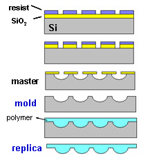
Replication techniques for micro and nano-optical components.
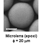
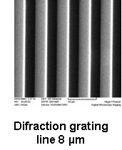
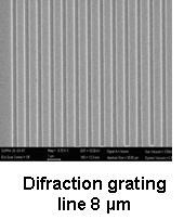
Development of replica molding techniques for replication of optical elements and microfluidic structures with feature size in the micron and submicron range.
 |

Lenses in epoxy resin obtained by replica molding with a master obtained by EBL in a) a thin layer of PMMA -950K layer; b) double PMMA layer (φ~150 nm, h ~200-300 nm)
|
 |
 |
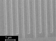
Microfluidic channels in PDMS width ~ 250 nm
|


