Structuring:
-
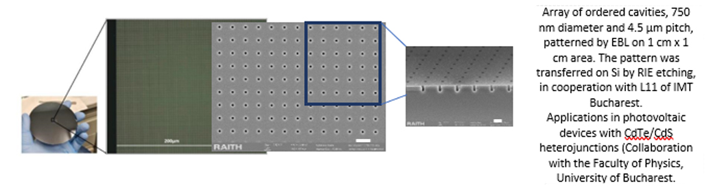
Nanoscale patterning by Gaussian e-beam lithography for applications in photonics, plasmonics, MSM-UV photodetectors, SAW components for RF/ microwave circuits etc.; Fabrication of graphene-based configurations and devices using EBL techniques.
Characterization:
-
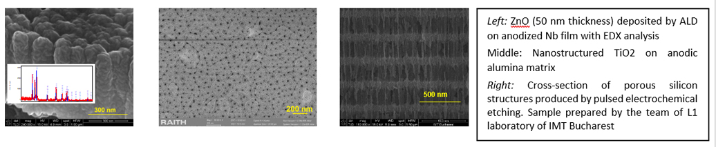
Field emission Scanning Electron Microscopy (FEG-SEM) and Energy Dispersive X-Ray Spectroscopy (EDX);
-
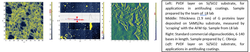
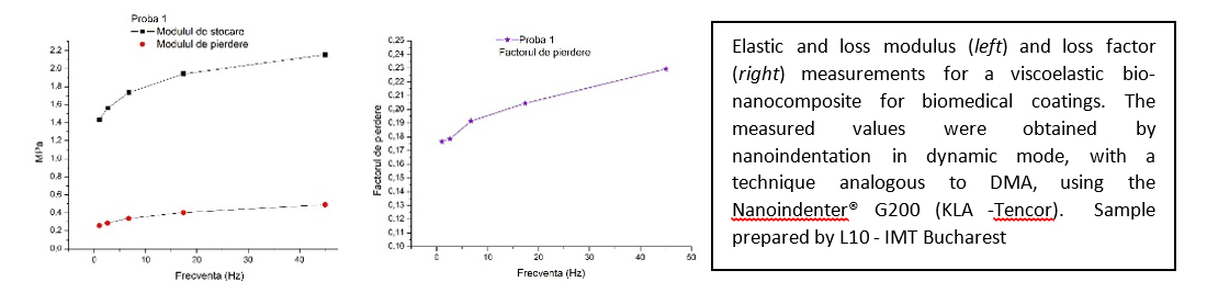
High-resolution surface and interface investigations by Scanning Probe Microscopy (SPM-AFM); Small-scale mechanical characterization using depth-sensing indentation (nano-indentation) testing.
Nanometric scale structuring by Electron Beam Lithography (EBL).
Contact: Dr. A. Dinescu, adrian.dinescu@imt.ro
Characterization (morphology, composition, material properties)
Scanning Electron Microscopy (FEG-SEM) with Energy Dispersive X-Ray Spectroscopy (EDX).
Contact: Dr. Oana Brîncoveanu, oana.brincoveanu@imt.ro, Phys. G. Crăciun, gabriel.craciun@imt.ro
Atomic Force Microscopy and related techniques (SPM).
Contact: Phys. R. Gavrilă, raluca .gavrila@imt.ro
Nano Indentation (Depth-sensing indentation techniques) for submicron scale mechanical characterization.
Contact: Phys. R. Gavrilă, raluca .gavrila@imt.ro
Education and training:
- Master courses and laboratory activities in collaboration with the University "Politehnica" of Bucharest:
“Advanced nanotechnological processes” - Master course, <<Microsystems>> MSc program, Faculty of Electronics, Telecommunications and Information Technology - ETTI, “Object-Oriented Programming” - Laboratory, Year II, ETTI, “Databases in Oracle environment” - Laboratory, Year III, <<Economical engineering in the electrical, electronic and energy fields>>, specialization, The Faculty of Entrepreneurship, Business Engineering and Management - FAIMA. |

