| |
|
| |
 Integrated Chips for biophotonics Integrated Chips for biophotonics |
| |
|
| |
Heterogeneous integration of polymeric waveguides with silicon photodiodes |
| |
| |
|
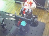
7.5 µm wide straight PMMA waveguide leacky-wave coupled with a Si photodiode – optical images and light propagation
|
Co-operation with Institute for Microstructure Technology (IMT), Forschungszentrum Karlsruhe (FZK), Germany |
|
|
| |
|
| |
SU-8 waveguide coupled with a silicon photodiode with a diffractive grating |
| |
|
| |
The optical coupling waveguide- photodiode is obtained with a grating realized in the bottom clading of the waveguide (pitch 4 µm).
The coupling eficiency depends on the refractive index of the surrounding media.
Applications: chemo and biosensors. |
|
|
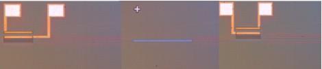
Optical image of the waveguide coupled with the photodiode |
Optical image: grating etched in SiO2 |
|
|
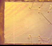
AFM image of the coupling region
(waveguide placed on the grating)
|
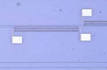
Image of the chip with bondig wires for the photodiode |
Co-operation with Institute for Microstructure Technology (IMT), Forschungszentrum Karlsruhe (FZK), Germany |
|
| |
|
| |
SU-8 waveguide coupled with a silicon photodiode |
| |
|
| |
The optical coupling waveguide- photodiode is obtained with a grating realized in the bottom clading of the waveguide (pitch 4 µm).
The coupling eficiency depends on the refractive index of the surrounding media.
Applications: chemo and biosensors. |
| |
Output waveguide coupled with photodiode |
Probe waveguide arm with sensing layer as cladding |
Y junction and reference photodiode coupled with the reference arm |
|
| |
SEM image of the coupling region (waveguide leacky-wave coupled with a Si photodiode)
|
|