|
| |
|
|
RESEARCH AREAS |
|
|
| |
Development of new technologies for rapid prototyping at micro-nanoscale |
|
| |
|
| |
 Dip pen nanolithography Dip pen nanolithography |
| |
|
| |
Is a nanolithography system that „prints” and „ink” directly on the substrate. The size of the geometrical features can vary from few tens of nanometers (in best conditions – 20 nm) up to several microns. It allows both a bottom-up approach and a top-down one when contructing the nanostructures.
|
| Some examples of applications of the dip pen nanolithography technique are presented below: |
-
surface functionalization (with direct liaison to proteomics, DNA recognition, virus identification);
-
photolithographic masks correction;
-
molecular electronics;
-
realization of master stamps for NIL (Nanoimprint lithography)
-
novel devices (photonic and electronic);
Image size is 5 microns x 5 microns, the width of the letters is 115 nm while the dot radius on top of letter “i” is 180 nm. Written with an organic acid (MHA) on gold substrate. Image was read by Atomic Force Microscopy at angle of 100 with respect to the writing direction. |
|
|
|
|
|
|
| |
|
| |
Design for and operation of 3D Printer based on Selective Laser Sintering |
| |
|
| |
 |
 |
 |
Moebius rings
(Phys. Eng. Victor Moagăr-Poladian)
|
Structure exhibiting negative Poisson coefficient
(courtesy of Phys. Eng. Victor Moagăr-Poladian) |
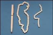
Bike mini-chains
(Eng. Dragoş Vârşescu, L7) |
| |
|
|
|
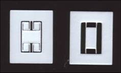
Image with two types of sensor structures. Left: optimized structure;
Right: usual structure central membrane is 1,5 cm.
The maximum size of the left structure |
Image showing the high deflection (~ 1.5 cm) of the optimized structure, pushed with the finger.
(Dr.Gabriel Moagăr-Poladian and
Phys. Eng. Victor Moagăr-Poladian)
|
|
|
| |
|
| |
Laser microengraving |
| |
|
| |
Results obtained with the system:
- Up to now we have used the system for engraving Si, Ge, thermally-grown SiO2, Cr/SiO2, glass, SiC.
- Nanoscale structures have been obtained, as presented in the next the images:
|
|
|
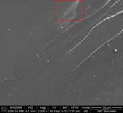
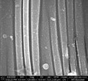
SEM image of the Si surface irradiated with high-power UV pulses.
The red rectangle is the region augmented in the central and left figures, respectively.
The Si wires have less than 130 nm diameter, are curved and form bundles.
Their lengths are between 10 microns and several tens of microns.The bar scale in the right image is of 400 nm.
|
|
|
|
|
|
|
|
| |
|
|
|
HOME |
 |
Last update:
February, 2012 |
|